
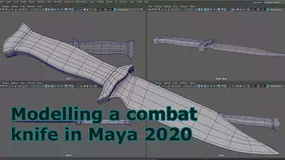
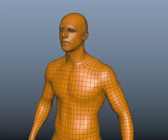
Introduction to Maya - Modeling Fundamentals Vol 1
This course will look at the fundamentals of modeling in Maya with an emphasis on creating good topology. We'll look at what makes a good model in Maya and why objects are modeled in the way they are.
#
31
04-12-2002
, 12:03 AM

Subscriber
Join Date: May 2002
Join Date: May 2002
Location: Faringdon, UK
Posts: 1,480
#
32
04-12-2002
, 12:37 AM

SM Alumni
Join Date: May 2002
Join Date: May 2002
Location: Exeter, UK
Posts: 407
 its the size at which the transistors are manufactured at.
 the more complex the chip (ie the greater the number of transistors), the greater the need to shrink the size of the transistors to avoid/reduce heat issues, and with the complexity of the NV30, nvidia had to make the transistors smaller, which as you can see isnt a cheap thing to do!
I'm no electrician/phycisist so this may not be totally accurate but i think its about right..
#
33
04-12-2002
, 12:44 AM
Subscriber
Join Date: May 2002
Join Date: May 2002
Location: Faringdon, UK
Posts: 1,480
its a bit stupid of nvidia, or any graphics card company to show off the gfx card by using the size of a component really! size does not matter
#
34
04-12-2002
, 12:49 AM

Subscriber
Join Date: Jul 2002
Join Date: Jul 2002
Posts: 1,253
hence the final result: FASTER AND ASS-KICKING PROCESSING!!!
#
35
04-12-2002
, 12:49 AM
SM Alumni
Join Date: May 2002
Join Date: May 2002
Location: Exeter, UK
Posts: 407
#
36
04-12-2002
, 12:58 AM
Subscriber
Join Date: May 2002
Join Date: May 2002
Location: Faringdon, UK
Posts: 1,480
#
37
04-12-2002
, 01:04 AM
Subscriber
Join Date: Jul 2002
Join Date: Jul 2002
Posts: 1,253
#
38
04-12-2002
, 01:05 AM
Subscriber
Join Date: Jul 2002
Join Date: Jul 2002
Posts: 1,253
so the first reason they did that is so that they can reduce heat, second it increases a bit of performance..
#
39
04-12-2002
, 01:06 AM

Registered User
Join Date: Sep 2002
Join Date: Sep 2002
Location: CCS, Venezuela
Posts: 3,363
Wouldn´t you?
adldesigner
Caracas, Venezuela
Hell .. not gone perse, but with a certainly lower post count per day.
#
40
04-12-2002
, 01:16 AM
Subscriber
Join Date: May 2002
Join Date: May 2002
Location: Faringdon, UK
Posts: 1,480
silly me <slaps himself> ow
#
41
04-12-2002
, 08:08 AM

Moderator
Join Date: Sep 2002
Join Date: Sep 2002
Location: London, UK
Posts: 3,198
#
42
04-12-2002
, 09:03 AM
SM Alumni
Join Date: May 2002
Join Date: May 2002
Location: Exeter, UK
Posts: 407
#
43
04-12-2002
, 01:23 PM
Subscriber
Join Date: May 2002
Join Date: May 2002
Location: Faringdon, UK
Posts: 1,480
#
44
04-12-2002
, 04:03 PM
Subscriber
Join Date: Jul 2002
Join Date: Jul 2002
Posts: 1,253
#
45
05-12-2002
, 01:06 AM

Subscriber
Join Date: Jul 2002
Join Date: Jul 2002
Location: MELville
Posts: 1,100
from what I head they spend $400,000,000 USD not 4 billionOriginally posted by kal
According to HardOCP (though not sure how much i trust this site...) Nvidia spent over 4 billion USD researching and developing the NV30

whatever they spent, it better be supa fast
(I head that it scored about 3 times better than the Wildcat 6210!!
 )
)-Emo
Posting Rules Forum Rules
Similar Threads
nVidia Quadro FX 1500 vs FX 1700
by Eelco in forum Maya Technical Issues replies 5 on 09-05-2008
Fx 5700 Ultra to Quadro FX 1100
by Phopojijo in forum Maya Basics & Newbie Lounge replies 0 on 16-06-2005
GeForce FX 5700 Vs. Radeon 9600 SE
by 13uRneR in forum Maya Technical Issues replies 8 on 11-12-2004
Geforce FX 5600?
by ragecgi in forum Maya Technical Issues replies 3 on 05-12-2003
48 days till Geforce FX?
by kbrown in forum Maya Basics & Newbie Lounge replies 14 on 24-01-2003
Topics


Free Courses


Full Courses


VFX News
How computer animation was used 30 years ago to make a Roger Rabbit short
On 2022-07-18 14:30:13
Sneak peek at Houdini 19.5
On 2022-07-18 14:17:59
VFX Breakdown The Man Who Fell To Earth
On 2022-07-15 13:14:36
Resident Evil - Teaser Trailer
On 2022-05-13 13:52:25
New cloud modeling nodes for Bifrost
On 2022-05-02 20:24:13
MPC Showreel 2022
On 2022-04-13 16:02:13